SC418
8
V
OUT
V
IN
+
CIN
Q2
+
D2
R
ILIM
C
BST
Q1
L
PGND
DL
ILIM
LX
DH
BST
C
OUT
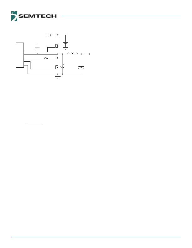
Figure 9 Valley Current Limit
Setting the valley current limit to 0A results in a peak
inductor current of 0A plus peak ripple current. In this
situation the average current through the inductor is 0A
plus one-half the peak-to-peak ripple current.
The R
ILIM
value is calculated by the next equation.
A
10
I
R
R
LIM
DSON
ILIM
The internal 0糀 current source is temperature compen-
sated at 400ppm in order to provide tracking with the
RDS
ON
.
Note that MOSFET RDS
(ON)
increases significantly if the
VDDP voltage is 3.3V compared to 5.0V. When selecting
the R
ILIM
value, use the RDS
(ON)
value that corresponds to
the VDDP voltage used in the application.
Soft-Start of PWM Regulator
Soft-start is achieved in the PWM regulator by using an
internal voltage ramp as the reference for the FB compara-
tor. The voltage ramp is generated using an internal
charge pump which drives the reference from zero to
500mV in .2mV increments, using an internal 500kHz
oscillator. When the ramp voltage reaches 500mV, the
ramp is ignored and the FB comparator switches over to a
fixed 500mV threshold. During soft-start the output
voltage tracks the internal ramp, which limits the start-up
inrush current and provides a controlled soft-start profile.
Typical soft-start ramp time is 850約.
During soft-start the regulator turns off the low-side
MOSFET on any cycle if the inductor current falls to zero,
regardless of the psave setting. This prevents negative
inductor current, allowing the device to start into a pre-
biased output.
Power Good Output
The PGOOD (power good) output is an open-drain output
which requires a pull-up resistor. When the voltage at the
FB pin is 0% below the nominal voltage, PGOOD is pulled
low. It remains low until the FB voltage returns above -8%
of nominal. During start-up PGOOD is held low and will
not be allowed to transition high until the PGOOD start-
up delay fime has passed and soft-start is completed
(when V
FB
reaches 500mV). The delay time starting from
EN going high is typically 2ms for VDDA = 5V and ms for
VDDA = 3.3V.
PGOOD will transition low if the FB voltage exceeds +20%
of nominal (600mV), which is also the over-voltage shut-
down threshold. PGOOD also pulls low if the EN pin is low
when VDDA is present.
Output Over-Voltage Protection
OVP (Over-voltage protection) becomes active as soon as
the device is enabled. The OVP threshold is set at 500mV
+ 20% (600mV). When V
FB
exceeds the OVP threshold, DL
latches high and the low-side MOSFET is turned on. DL
remains high and the controller remains off until the EN
input is toggled or VDDA is cycled. There is a 5約 delay
built into the OVP detector to prevent false transitions.
PGOOD is also low after an OVP event.
Output Under-Voltage Protection
When V
FB
falls 25% below its nominal voltage (falls to
375mV) for eight consecutive clock cycles, the switcher is
shut off and the DH and DL drives are pulled low to tri-
state the MOSFETs. The controller stays off until EN is
toggled or VDDA is cycled.
VDDA UVLO and POR
The VDDA Under-Voltage Lock-Out (UVLO) circuitry inhib-
its switching and tri-states the DH/DL drivers until VDDA
rises above 2.9V. When VDDA exceeds 2.9V, an internal
POR (Power-On Reset) resets the fault latch and the soft-
start counter and then the SC48 begins the soft-start
Applications Information (continued)
发布紧急采购,3分钟左右您将得到回复。
相关PDF资料
SC424MLTRT
IC REG DL BUCK/LINEAR 28MLPQ
SC4250LISTRT
IC HOT SWAP CTRLR 8-SOIC
SC427MLTRT
IC REG DL BUCK/LINEAR 32MLPQ
SE95D,112
IC SENSOR TEMP 2.8-5.5V SOT96-1
SE97BTP,547
IC TEMP SENSOR DIMM 8HWSON
SE98ATP,547
IC TEMP SENSOR DDR 8-HWSON
SG6901ASZ
IC PFC CTLR AVERAGE CURR 20SOIC
SG6932SZ
IC PFC CONTROLLER CCM 16SOP
相关代理商/技术参数
SC419
制造商:SEMTECH 制造商全称:Semtech Corporation 功能描述:EcoSpeedTM DC-DC Converter with Integrated Boost Diode
SC419970CGCR2
制造商:Motorola Inc 功能描述:
SC419EVB
制造商:SEMTECH 制造商全称:Semtech Corporation 功能描述:EcoSpeedTM DC-DC Converter with Integrated Boost Diode
SC419ULTRT
功能描述:IC REG CTRLR BUCK PWM 20-MLPQ RoHS:是 类别:集成电路 (IC) >> PMIC - 稳压器 - DC DC 切换控制器 系列:EcoSpeed®, SmartDrive™ 特色产品:LM3753/54 Scalable 2-Phase Synchronous Buck Controllers 标准包装:1 系列:PowerWise® PWM 型:电压模式 输出数:1 频率 - 最大:1MHz 占空比:81% 电源电压:4.5 V ~ 18 V 降压:是 升压:无 回扫:无 反相:无 倍增器:无 除法器:无 Cuk:无 隔离:无 工作温度:-5°C ~ 125°C 封装/外壳:32-WFQFN 裸露焊盘 包装:Digi-Reel® 产品目录页面:1303 (CN2011-ZH PDF) 其它名称:LM3754SQDKR
SC41E6
制造商:INFINEON 制造商全称:Infineon Technologies AG 功能描述:SIEMENS ANNOUNCES A SUB-MICTON GENERATION OF CHANNELLESS GATE-ARRAYS BASED ON THE PROVEN MEGALOGIC PROCESS
SC4-2 24VDC
制造商:PEPPERL+FUCHS 功能描述:Sensor, Machine Safety, Control Unit, 24VDC, 2 Channel, LED Display, 117230
SC420
功能描述:UPS - 不间断电源 420VA/260W 4 Outlet
RoHS:否 制造商:Phoenix Contact 功率额定值: 输出电压额定值:24 V 出口数量:2 运行时间(满载): 运行时间(半载):
SC4201
制造商:SEMTECH 制造商全称:Semtech Corporation 功能描述:Multi-Phase Link Controller
